1 Errata
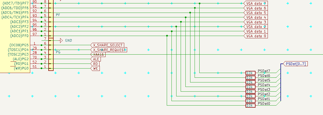
- all 10 kΩ resistors in PS/2 (8+2) should be rather 1 kΩ (otherwise it take too long for reading values, like 10 clock cycles)
2 PS/2
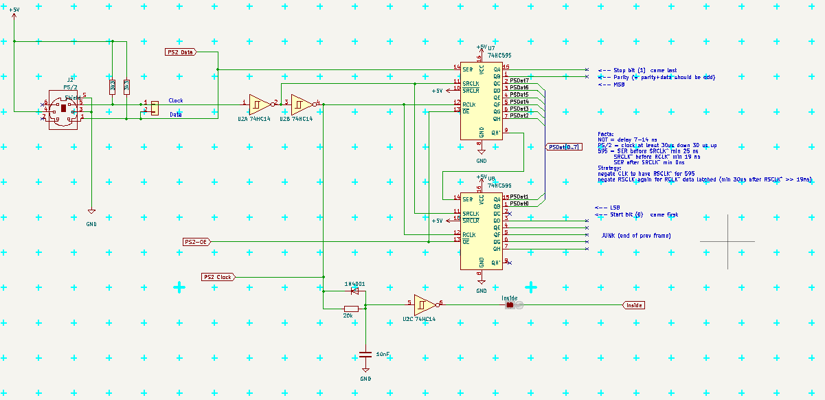
PS/2 have 2 lines - Clock and Data. See https://wiki.osdev.org/PS/2_Keyboard
Clock runs at 10-17 kHz, 11 pulses (normal High, active LOW), data came as
- 1 start bit (always 0)
- 8 data bits (least significant bit first)
- 1 parity bit (odd parity)
- 1 stop bit (always 1)
The clock/data can be connected directly to PB2/PB3 MOSI/MISO via solder jumpers (default OPEN, solder to USE) and decoded as serial communication, but I will use two shift registers and R-C to detect, if we are Inside the packet or not, so I could read the data as one byte on port PF, when I do not use it as VGA data output.
Inside signal (connected via closed solder jumper, cut if not wanted) is HIGH when clock is changing, LOW, when clock stops and PSDat is valid.
PS-OE is active LOW and let the captured PS data go to port PF
(In next version I may redirect PS Clock BEFORE fixing its edges by Schmitt 74HC14, so it would be possible also send data like status LEDs (Caps,Num,Scrl) to keyboard)
The plan is to check at end of VGA line, if the Inside went LOW, then set port PF ro read, set PS2-OE LOW, read PF and set PS2-OE HIGH again. Inside is way longer than VGA line and pause between two PS/2 blocks is also long enought for it.
The schema is distributed over more places.
The main part with shift registers:
Connection to data:
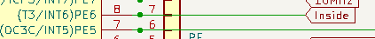
Inside signal:
Serial clock+data signals:

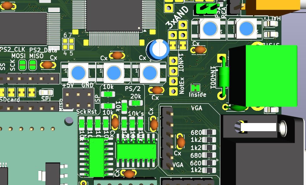
Top PCB:
Bottom:
