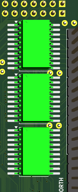
1 RAM (External + Shared)
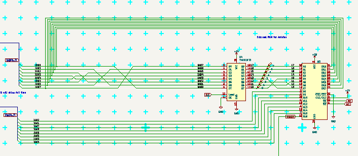
External RAM may be used to have visible 64kB RAM inside MCU (but those 56kB extra is 1 tick slower to access).
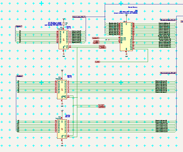
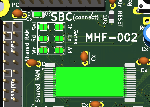
Shared RAM may be shared with retrocomputer or used as just storage with slower time then RAM but faster then anything else.
Both are 128kB chips CY7C109D, as I found them to be cheap, accessible and 5V friendly. The truth is, that their output is lower then 3.4V, but Atmega should be able use it anyway. 74HC245 gate may need power little lower than +5V, so I added resistor there to slightly decrease it (or maybe Schottky diode). I will see, if it is really needed.
Note that near the RAM datalines may be permutated any way, as well as adderss lines, because it does not matter, the permutation will negate when the data are readed back. So it may be used to have better physical traces there (as I did).
External RAM is connected to ports PA and PC, where PA is latched by 74AHC573 fast octal D-latch. It must be enabled in SW and managed by PG0-2. I will use PG3 to select in which half of chip it resides.
It can be accessed also manually if the automatic is not enabled, by setting low address to PA, latch it and then use PA as data line. This way any byte in 128kB may be used at slower access time. I will probabely use it for futher expansion of FORTH memory. those 8 squares around it are probes of D-latch output, so it could be tested too. D-latch is placed under the PCB to have short lines to RAM.
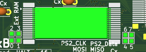
Shared RAM is connected to ports PJ, PK and PL, and in graphic card configuration is managed in cooperation with GLUE. In SBC configuration the MCU need to manage it itself, so all SBC solder jumpers should be soldered. If output to System Bus is not needed, also gates may be unpopulated.